
Electron Microscopy introduction
Electron microscopy uses an electron beam to create an image of a sample. Because of this an electron microscope has a much greater resolving power than a light microscope and is capable of much highermagnifications (up to 2 million times).
There are two types of electron microscopes - transmission electron microscopes (TEM) and scanning electron microscopes (SEM). SEM shows the specimen surface, TEM is used to reveal structures of thin samples or thin sections. TEM images are two-dimensional projections of 3D objects. Electron microscopy can be used to investigate the microstructure of a wide range of biological and inorganic specimens providing morphologic and crystallographic information. The EM operates under vacuum which means the samples are placed in a vacuum system during analysis. Therefore, some samples need to be specially prepared to withstand the environment inside an electron microscope.
Transmission Electron Microscopy
In transmission electron microscopy (TEM) a beam of electrons is transmitted through a thin specimen to form an image. After magnification the image is projected onto a fluorescent screen or a digital camera.

The details that TEM can reveal are very fine, almost molecular in spatial resolution. For objects like viruses, nanoparticles or polymer aggregates hardly any preparation is necessary. Larger structures are usually cut in thin sections (<100nm) to make them transparent for the electron beam. All samples need to be placed on 3 millimeter discs (grids) with a fine mesh. TEM allows imaging of the structure of a wide range of samples from biological, medical, and materials sciences.
WEMC has two Transmission Electron Microscopes which offer the following features:
- Standard TEM
- High-resolution TEM
- Tomography/Three dimensional imaging
- Cryo-TEM
- Negative staining electron microscopy
- Immuno electron microscopy
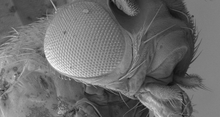
Scanning Electron Microscopy
In a scanning electron microscope (SEM) an electron beam is scanning in a raster pattern over the sample. The electrons interact with atoms in the sample and the secondary electrons emitted by the sample are used to form an image of the sample surface. The SEM at WEMC is a FEI Magellan 400, with an electron energy range from 1 kV to 30 kV and a sub-nanometer resolution (0.8 nm at 15 kV—0.9 nm at 1 kV).

CRYO-SEM
The FEI Magellan 400 is equipped with a Leica cold stage for cryo-microscopy. Low-temperature SEM can be performed on frozen material.
Energy-dispersive X-ray spectroscopy EDX-SEM
During SEM imaging X-rays are emitted from the sample. Interaction of the electron beam with atoms in the sample causes shell transitions which result in the emission of X-rays. An emitted X-ray beam has an energy which is characteristic of the parent element. Determining the emitted X-ray energies can be used for the quantitative elemental analysis of the sample. Energy-dispersive X-ray spectroscopy (EDX) can also be used to form maps or line profiles, showing the elemental distribution in a sample surface (sampling depth 1-2 microns).